AFMシステム
アクセサリ
アプリケーション
お問い合わせ
キャンペーン
「AFMプローブ」 プレゼント
 オックスフォード・インストゥルメンツー事業部ページ

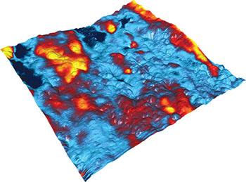
原子間力顕微鏡 (AFM, atomic force microscopy) は、高い空間分解能および直接的なプロービング機能により、ナノスケールの電気的な特性を評価するための強力なツールとなります。アサイラム・リサーチでは、ナノスケールの電気特性を評価するためのツール一式を MFP-3D™ AFMファミリーおよびCypher™ AFMファミリーで提供しています。定量的な電気的測定を目的としていますが、電気特性評価モード(エレクトリカルモード)は、サンプル中の物質を、電気特性の定性的な相違に基づいて比較し、その成分の検出・識別・同定をすばやく行うためにも頻繁に使用されます。
Cypher AFM用のレーザー干渉変位計測オプション(IDS, Interferometric Displacement Sensor)を使用することにより、圧電応答顕微鏡 (PFM, piezoresponse force microscopy) を使用したd33値測定の再現性が高まり、アーティファクトを取り除くことができます。IDSは、従来の光てこによるたわみ検出法(OBD, optical beam deflection)に利用されるカンチレバー角度の代わりに、カンチレバーのたわみを直接測定します。 IDSは、静電相互作用によるアーティファクトを除去します。 下の技術資料のタブより、IDSオプションのデータシートをダウンロードしていただけます。
"Local characterization of mobile charge carriers by two electrical AFM modes: multi-harmonic EFM versus sMIM," L. Lei, R. Xu, S. Ye, X. Wang, K. Xu, S. Hussain, Y. J. Li, Y. Sugawara, L. Xie, W. Ji, and Z. Cheng, J. Phys. Commun. 2, 025013 (2018). https://doi.org/10.1088/2399-6528/aaa85f
"Probing the ionic and electrochemical phenomena during resistive switching of NiO thin films," W. Lu, J. Xiao, L.-M. Wong, S. Wang, and K. Zeng, ACS Appl. Mater. Interfaces 10, 8092 (2018). https://doi.org/10.1021/acsami.7b16188
"Optimization of the Ag/PCBM interface by a rhodamine interlayer to enhance the efficiency and stability of perovskite solar cells," J. Ciro, S. Mesa, J. I. Uribe, M. A. Mejía-Escobar, D. Ramirez, J. F. Montoya, R. Betancur, H.-S. Yoo, N.-G. Park, and F. Jaramillo, Nanoscale 9, 9440 (2017). https://doi.org/10.1039/c7nr01678f
"Spatially resolved multicolor CsPbX3 nanowire heterojunctions via anion exchange," L. Dou, M. Lai, C. S. Kley, Y. Yang, C. G. Bischak, D. Zhang, S. W. Eaton, N. S. Ginsberg, and P. Yang, Proc. Natl. Acad. Sci. U.S.A. 114, 7216 (2017). https://doi.org/10.1073/pnas.1703860114
"New insights on electro-optical response of poly(3,4-ethylenedioxythiophene):poly(styrenesulfonate) film to humidity," E. S. Muckley, C. B. Jacobs, K. Vidal, J. P. Mahalik, R. Kumar, B. G. Sumpter, and I. N. Ivanov, ACS Appl. Mater. Interfaces 9, 15880 (2017). https://doi.org/10.1021/acsami.7b03128
"Mapping the photoresponse of CH3NH3PbI3 hybrid perovskite thin films at the nanoscale," Y. Kutes, Y. Zhou, J. L. Bosse, J. Steffes, N. P. Padture, and B. D. Huey, Nano Lett. 16, 3434 (2016). https://doi.org/10.1021/acs.nanolett.5b04157
"Grain boundary dominated ion migration in polycrystalline organic–inorganic halide perovskite films," Y. Shao, Y. Fang, T. Li, Q. Wang, Q. Dong, Y. Deng, Y. Yuan, H. Wei, M. Wang, A. Gruverman, J. Shield, and J. Huang, Energy Environ. Sci. 9, 1752 (2016). https://doi.org/10.1039/c6ee00413j
"High‐performance and environmentally stable planar heterojunction perovskite solar cells based on a solution‐processed copper‐doped nickel oxide hole‐transporting layer," J. H. Kim, P.‐W. Liang, S. T. Williams, N. Cho, C.-C. Chueh, M. S. Glaz, D. S. Ginger, and A. K.‐Y. Jen, Adv. Mater. 27, 695 (2015). https://doi.org/10.1002/adma.201404189
"Gate-tunable memristive phenomena mediated by grain boundaries in single-layer MoS2," V. K. Sangwan, D. Jariwala, I. S. Kim, K. S. Chen, T. J. Marks, L. J. Lauhon, and M. C. Hersam, Nat. Nanotechnol. 10, 403 (2015). https://doi.org/10.1038/nnano.2015.56
"Polymer homo‐tandem solar cells with best efficiency of 11.3%," H. Zhou, Y. Zhang, C. K. Mai, S. D. Collins, G. C. Bazan, T. Q. Nguyen, and A. J. Heeger, Adv. Mater. 27, 1767 (2015). https://doi.org/10.1002/adma.201404220
"Observation and alteration of surface states of hematite photoelectrodes," C. Du, M. Zhang, J.-W. Jang, Y. Liu, G.-Y. Liu, and D. Wang, J. Phys. Chem. C 118, 17054 (2014). https://doi.org/10.1021/jp5006346
"Solvent‐polarity‐induced active layer morphology control in crystalline diketopyrrolopyrrole‐based low band gap polymer photovoltaics," S. Ferdous, F. Liu, D. Wang, and T.P. Russell, Adv. Energy Mater. 4, 1300834 (2014). https://doi.org/10.1002/aenm.201300834
"Quantifying charge carrier concentration in ZnO thin films by scanning Kelvin probe microscopy," C. Maragliano, S. Lilliu, M. S. Dahlem, M. Chiesa, T. Souier, and M. Stefancich, Sci. Rep. 4, 4203 (2014). https://doi.org/10.1038/srep04203
"A new quantitative experimental approach to investigate single cell adhesion on multifunctional substrates," C. Canale, A. Petrelli, M. Salerno, A. Diaspro, and S. Dante, Biosens. Bioelectron. 48, 172 (2013). http://doi.org/10.1016/j.bios.2013.04.015
"Kelvin probe microscopy and electronic transport measurements in reduced graphene oxide chemical sensors," C. E. Kehayias, S. MacNaughton, S. Sonkusale, and C. Staii, Nanotechnology 24, 245502 (2013). https://doi.org/10.1088/0957-4484/24/24/245502
"High spatial resolution Kelvin probe force microscopy with coaxial probes," K. A. Brown, K. J. Satzinger, and R. M. Westervelt, Nanotechnology 23, 115703 (2012). https://doi.org/10.1088/0957-4484/23/11/115703
"Sub-30 nm scaling and high-speed operation of fully-confined access-devices for 3D crosspoint memory based on mixed-ionic-electronic-conduction (MIEC) materials," K. Virwani, G.W. Burr, R.S. Shenoy, C.T. Rettner, A. Padilla, T. Topuria, P.M. Rice, G. Ho, R.S. King, K. Nguyen, A.N. Bowers, M. Jurich, M. BrightSky, E.A. Joseph, A.J. Kellock, N. Arellano, B.N. Kurdi, and K. Gopalakrishnan Kumar, in IEEE International Electron Devices Meeting 2012 Technical Digest (10-13 December 2012, San Francisco, CA), pp. 2.7.1-2.7.4. https://doi.org/10.1109/iedm.2012.6478967
"Photoinduced degradation studies of organic solar cell materials using Kelvin probe force and conductive scanning force microscopy," E. Sengupta, A. L. Domanski, S. A. Weber, M. B. Untch, H. J. Butt, T. Sauermann, H. J. Egelhaaf, and R. Berger, J. Phys. Chem. C 115, 19994 (2011). https://doi.org/10.1021/jp2048713
"Kelvin force microscopy studies of work function of transparent conducting ZnO:Al electrodes synthesized under varying oxygen pressures," R. Jaramillo and S. Ramanathan, Sol. Energy Mater. Sol. Cells 95, 602 (2011). https://doi.org/10.1016/j.solmat.2010.09.025
"Nanoscale, electrified liquid jets for high-resolution printing of charge," J.-U. Park, S. Lee, S. Unarunotai, Y. Sun, S. Dunham, T. Song, P. M. Ferreira, A. G. Alleyene, U. Paik, and J. A. Rogers, Nano Lett. 10, 584 (2010). https://doi.org/10.1021/nl903495f
"Highly efficient solar cell polymers developed via fine-tuning of structural and electronic properties," Y. Liang, D. Feng, Y. Wu, S.-T. Tsai, G. Li, C. Ray, and L. Yu, J. Am. Chem. Soc. 131, 7792 (2009). https://doi.org/10.1021/ja901545q
"Differential conductivity in self-assembled nanodomains of a diblock copolymer using polystyrene-block-poly(ferrocenylethylmethylsilane)," J. K. Li, S. Zou, D. A. Rider, I. Manners, and G. C. Walker, Adv. Mater. 20, 1989 (2008). https://doi.org/10.1002/adma.200702796
"Space charge limited current measurements on conjugated polymer films using conductive atomic force microscopy," O. G. Reid, K. Munechika, and D. S. Ginger, Nano Lett. 8, 1602 (2008). https://doi.org/10.1021/nl080155l
"Near-static dielectric polarization of individual carbon nanotubes," W. Lu, D. Wang, and L. Chen, Nano Lett. 7, 2729 (2007). https://doi.org/ 10.1021/nl071208m
"Piezoelectric and semiconducting coupled power generating process of a single ZnO belt/wire. A technology for harvesting electricity from the environment," J. Song, J. Zhou, and Z. L. Wang, Nano Lett. 6, 1656 (2006). https://doi.org/10.1021/nl060820v

© オックスフォード・インストゥルメンツ 2026